Make a call
+86 13043405011
Make a call
+86 13043405011
|
Process |
English |
Applicable Components |
Features |
Typical Applications |
|
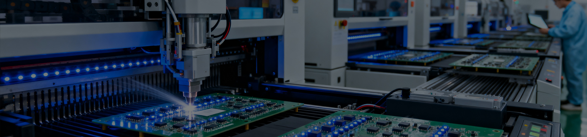
Surface Mount Technology |
SMT |
Chip resistors/capacitors, ICs, BGA, diodes |
Small size, high density, high automation |
Mobile phones, computers, consumer electronics |
|
Through-Hole Technology |
THT |
Connectors, electrolytic capacitors, transformers, high-power devices |
High mechanical strength, suitable for high current/high power |
Power supplies, industrial control, home appliances |
|
Hybrid Technology |
SMT+THT |
Both SMT and through-hole components on the board |
Balances high density and strong connection |
Most modern electronic products |
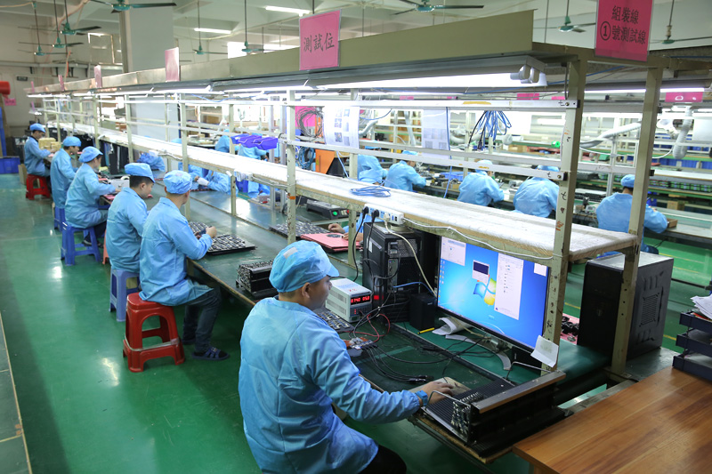
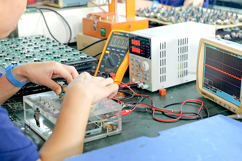
The company integrates complete design and development, manufacturing, and international trade import and export.